Lexicon 480L digital reverb — Audio glitches
Table of Contents
Hear the Gear #
What’s on the Bench #
The Lexicon 480L is an established legend in the world of digital reverberation. Released in 1986, it is a staple of lush, dense reverbs that infuse many 80s and 90s albums. It’s been such a famous piece of gear that many emulations are now available as DAW plugins.
The effects unit is composed of two subunits:
- Mainframe: a 3U rack-mounted processing module, which hosts the motherboard, the Host Processor Board (CPU), the memory cartridge, and the two High Speed Processors (HSP1 and HSP2). Some rare units also include the Sampling Memory Expander (SME), providing up to 23.7 s of additional sampling memory.
- LARC: the iconic Lexicon Alphanumeric Remote Control unit.

The motherboard is in charge of the A/D and D/A conversions, the Host Processor Board controls the presets and the parameters, and the two HSP boards are the digital audio processing kernels. Each HSP hosts a dedicated processor, a bank of DRAM to store the audio buffers, and all the logic to process the audio streams: the equivalent of a modern DSP chip, but at a lower hardware level, implemented with Z80 and 68k microprocessors and a whole bunch of discrete DIP-package logic integrated circuits.
Issue Localization #
The unit on the bench today is suffering from a rhythmic glitch on the output signal. This is a strong indication of a possible audio DRAM chip failure on one of the HSP boards. The audio DRAM on these boards is composed of a bank of 41464-10 chips that act as a circular buffer for storing the digital audio data during the processing.
The 41464-10 is a 64K × 4-bit Dynamic RAM (DRAM) IC in an 18-pin DIP package, operating on a single +5 V rail. The -10 suffix indicates a maximum access time of 100 ns.
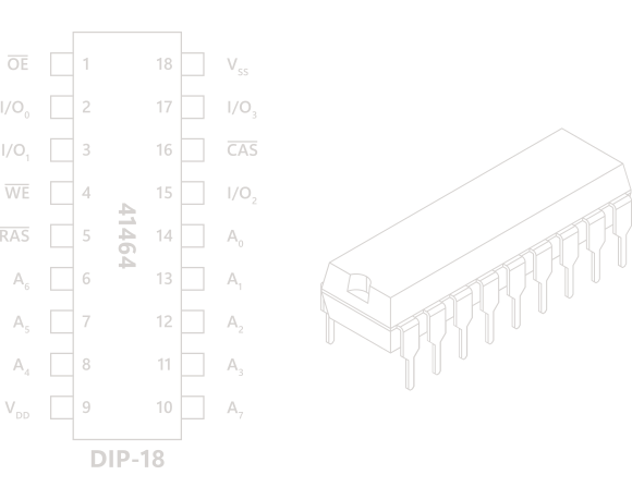
This memory chip is, of course, discontinued, and as such, it has become pretty rare nowadays. It is often sought after by retro-computing enthusiasts since it was used a lot in later revisions of the Commodore 64C.
Each HSP board has two banks of five DRAM ICs (Designators U64-68 and U93-97), one for the left and the other for the right audio channel, for a total of 20 chips per machine. Due to the rarity of the IC, it makes no sense to blindly swap all 20 ICs. It would be a total waste of money and time.
Unfortunately, though, it is not easy to localize the actual faulty chip because the board is not accessible for probing when plugged into the main rack assembly. The best compromise in terms of cost/risk is to isolate which of the four banks of RAM is affected and swap it altogether.
A simple three-step procedure can be used to pinpoint the origin of the failure, reducing the number of swapped ICs from 20 to 5.
Isolate the Faulty HSP Board #
The unit is populated with only one HSP card at a time. As the internal slots are fully interchangeable, the operating system automatically configures the unit for single-machine operation. Each board is tested individually to identify which card triggers the system fault.
Configure the Diagnostic Preset #
A Twin Delays preset (Bank 6) is selected and configured for full L/R panning with zero cross-feedback. On Page 3 of the LARC interface, the cross-feedback paths are disabled by setting parameters FB3, LV3, FB4, and LV4 all to 0.
Pinpoint the Defective DRAM Bank (L vs. R) #
Left and Right output channels are monitored independently while passing audio through the diagnostic preset. The channel producing the glitch pinpoints the failure directly to the corresponding DRAM bank on the active HSP board.
Following these steps allowed the failure to be pinpointed to the L channel of HSP1, requiring the substitution of the U64-68 bank.
Sourcing DRAM Chips #
The affected IC has been produced by many major semiconductor manufacturers, and being a DRAM, it is always drop-in thanks to JEDEC standards. The only significant detail to consider is the access time, which must be 100 ns or lower.
| Manufacturer | Direct Drop-In Part Number |
|---|---|
| NEC | uPD41464C-10 D41464C-10 |
| Texas Instruments | TMS4464-10NL TMS4464JL-10 |
| Hitachi | HM50464P-10 HM51464P-10 |
| Fujitsu | MB81464-10 |
| Samsung | KM41464-10 |
| Hyundai | HY534464-10 HY53C464LS-10 |
| Panasonic / Matsushita | MN41464A-10 MN41464A-08 |
| Motorola | MCM61464-10 |
The Suffering #
Purchasing discontinued and/or rare chips is always a pain in the arse. AliExpress or eBay listings are notorious for counterfeit IC sellers. Usual reputable suppliers (Mouser, Digikey, RS Components, many others…) do not stock the obsolete DRAM. Using disassembled parts from other machines was also non-viable due to the unknown usage and state of the ICs.
After a month-long search among minor electronic suppliers all over Europe and on multiple obscure retro-computing forums, no supplier nor website gave me enough confidence, and I was starting to hit a dead end.
The Breakthrough #
Fortunately, through some acquaintances, I got in contact with a very wholesome guy who worked for the Italian Lexicon division in the 90s. He very kindly asked the manufacturer directly about the availability of some original ICs, and he was able to source not only the 5 required ICs but a full batch of 20 original, still sealed, NOS, HY53C464LS-10 DRAM chips. Turns out, having an insider contact in your phonebook is basically a real-life cheat code for striking vintage silicon gold!
Replacement Procedure #
With the HSP1 board finally on the bench, the actual repair can start. First step requires a good amount of flux to be applied on the pins that need desoldering.
Using a 380 °C preheated desoldering gun, all 90 pins of the 5 DRAM chips are carefully unsoldered. The tip must be placed on the pad, a few seconds are needed for the solder to completely melt, and then a small wiggle is applied to the tip of the gun in order to free up the pin. While still wiggling the pin, the vacuum is activated until the suction of all the molten solder is completed.
After all pins are completely freed from solder alloy, each pin is again gently wiggled with a fine-point tweezers to completely detach it from the pad walls. After each pin is free to move, small pliers are used to extract the IC.
A high-quality, gold-plated, turned IC socket is inserted in place of each of the DRAMs, and it is resoldered back to the board.
The brand-new ICs are finally carefully inserted into the sockets, observing the correct position of Pin 1, marked by the notch on the chip.

Final Test #
The unit is fully populated with both HSP boards and tested using a few presets from each bank. The issue is completely resolved, and the unit can go back to churning out its luxurious, 80s-style reverb tails.